Introduction
This tutorial example demonstrates simulation of a ring resonator. This type of integrated photonic device is e.g. used as add/drop filter, or in applications for sensing, where substances or particles are detected by measuring a shift of the resonance frequency of the ring when they attach to it:
For passive optical devices in integrated photonic circuits, often the S-matrix is of interest. It describes how electromagnetic fields entering the device via its ports/waveguides propagate to all ports of the device. The entries of the S-matrix are complex numbers inheriting amplitude change and phase shift of the field. A complete network of devices is usually simplified by computing all S-matrices of the involved structures and then solving a globally coupled S-matrix for the circuit.
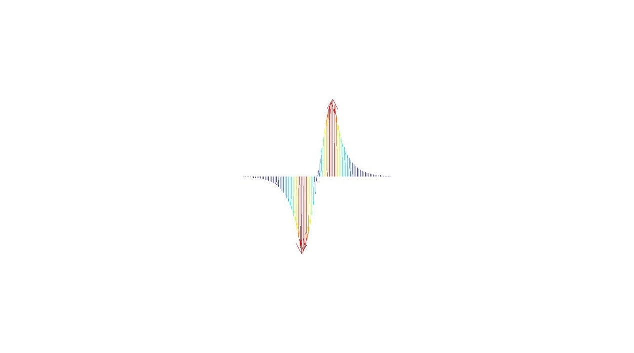
This type of scattering simulation of above device involves two steps. First, waveguide modes entering the device are computed. These are not analytical solutions like plane wave sources, therefore they are obtained numerically using FEM. For the 2D ring resonator example, 1D propagating modes are computed (slab waveguide modes).
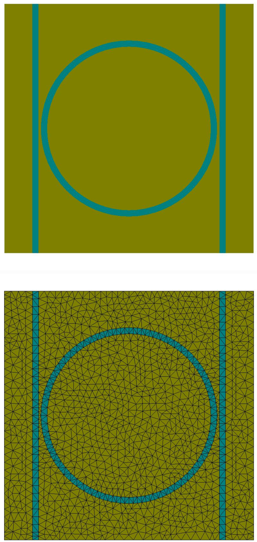
In this example, all waveguides entering the device have the same geometry. The 2D geometry is set up by the assembly of the circular ring resonator, and two parallel waveguides:
Layout2D {
Name = "Ring_Resonator"
UnitOfLength = 1e-06
MeshOptions {
MaximumSideLength = 0.5
}
Objects {
Polygon {
Name = "ComputationalDomain"
Points = [-6 -6
-3 -6
6 -6
6 6
-6 6]
DomainId = 1
Priority = -1
Boundary {
Class = Transparent
BoundaryId = 1
Number = 1
}
Boundary {
Class = Transparent
Number = [2 3 4 5]
}
}
Parallelogram {
Name = "Waveguide1"
Width = 0.3
Height = 12
GlobalPosition = [4.5 0.0]
DomainId = 2
Priority = 2
}
Parallelogram {
Name = "Waveguide2"
Width = 0.3
Height = 12
GlobalPosition = [-4.5 0.0]
DomainId = 2
Priority = 2
}
Circle {
Name = "CircleInner"
DomainId = 1
Priority = 3
RefineAll = 3
Radius = 3.94
}
Circle {
Name = "CircleOuter"
DomainId = 2
Priority = 2
RefineAll = 3
Radius = 4.24
}
}
}
Source mode computation
In order to extract the 1D geometry of a single waveguide, the lower boundary of the computational domain is defined by two segments ranging from to and from to . The boundary ranging from to is marked by BoundaryId = 1. In the sub folder 1D which includes simulation files for the propagating mode problem, the layout is defined by:
ExtractFace{
InputFileName="../grid.jcm"
BoundaryId=1
CoordinateSystem=Local
}
This extracts the marked boundary with BoundaryId = 1 from the 2D mesh and creates the corresponding 1D mesh. The boundary end points of this 1D mesh are also given the same BoundaryId, which is used in the boundary_conditions.jcm file to define tangential electric boundary conditions. An image of the 1D mode is shown below:
Scattering matrix computation
Once the 1D propagating mode is computed it can be used as a source in the 2D simulation, as defined in sources.jcm:
MultipleSources {
PropagatingModes {
DetectPorts = yes
FileName = "./1D/project_results/fieldbag.jcm"
}
}
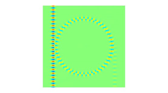
This so-called MultipleSource performs the coordinate transformation of the 1D solution to the extracted port automatically. Further, when DetectPorts = yes is set, the boundary of the device is scanned to find matching in-going waveguide structures, and the computed 1D mode is set as independent source at each port. When solving the 2D problem, therefore 4 fields are computed - one for each port. The post-process ModeOverlap computes the entries of the scattering matrix. Here, the computed 1D modes are specified by ModeFileName to project the scattering onto these modes. Again, all ports of the geometry which match the 1D grid are determined automatically, and a 4x4 S-matrix is computed. Because of the symmetry of the device, also the S-matrix exhibits symmetries, up to the numerical accuracy.
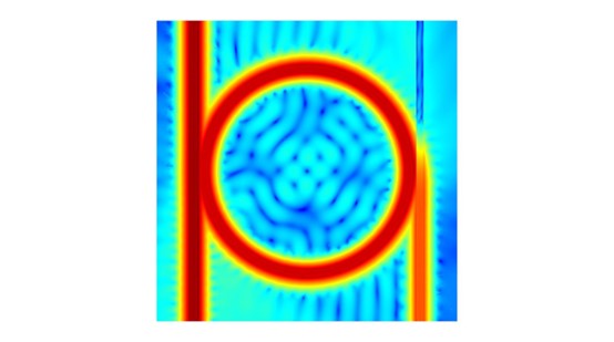
Below, the x-component of the electric near-field and the logarithm of the light intensity are shown:
|